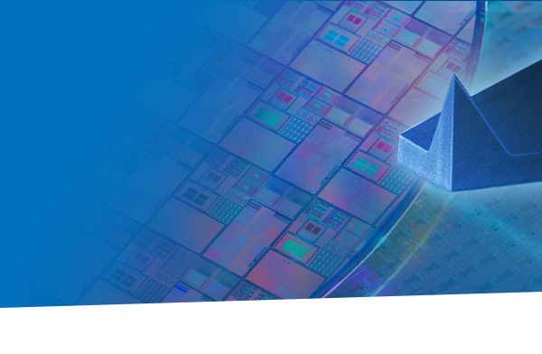
Atomic Force Microscopy for Advanced Surface Characterization and Metrology for the Semiconductor Industry
Tuesday, April 16 | 8AM PDT | 11AM EDT | 5PM CEST
Join us for this live webinar on advanced surface characterization and metrology solutions for the semiconductor industry. Learn about the techniques available for in-line process control and the nanoscale characterization of the topography and advanced physical properties of semiconductor materials and devices.
Bruker’s atomic force microscopy (AFM)-based techniques set industry-leading standards, delivering highest accuracy and non-destructive, high-throughput solutions for R&D and fully automated in-line process control.
In this webinar, we will illustrate how AFM can be applied in modern node and wafer processing steps and front-end/back-end applications to achieve actionable data and enhanced yield. We will provide an overview of high-resolution imaging, profiling, and metrology techniques, illustrated with a variety of case studies.
Topics will include:
- Assessment of surface roughness, bonding/hybrid bonding applications, and CMP processes
- Large-scale metrology on the millimeter scale, for full die, field effect, and bevel edges
- Critical dimension (CD) and sidewall metrology of lines, trenches, and vias
- Fully automated characterization of mechanical and electrical properties, carrier profiling, reliability testing, and failure analysis of nanoscale defects on blanket and patterned wafers
- Photothermal NanoIR spectroscopy for chemical identification and mapping on the nanoscale
- AFM-based defect manipulation and repair for photomask
Don’t miss the opportunity to speak to our experts in the Q&A session!
Visit the Bruker Wepage to see all of our solutions for semiconductor manifacturing.
Meet the Bruker Team

Dr. Ingo Schmitz (Chair)
Senior Technical Marketing

Dr. Peter De Wolf
Senior Director Technology & Applications AFM

Sean Hand
Senior Staff Applications Scientist Semiconductors
Meet the Bruker Team
Dr. Ingo Schmitz (Chair)
Senior Technical Marketing
Dr. Peter De Wolf
Senior Director Technology & Applications AFM
Sean Hand
Senior Staff Applications Scientist Semiconductors


