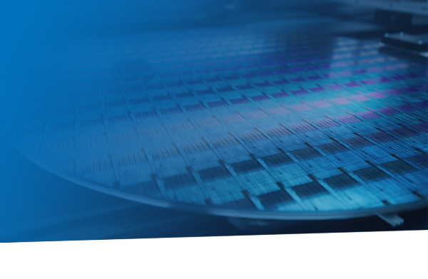
Atomic Force Microscopy Methods for Semiconductor Failure Analysis
Wednesday, May 28 | 8AM PDT | 11AM EDT | 5PM CEST
Atomic force microscopy (AFM) is well known for its standard capability to image surface topography with nanometer-scale spatial resolution. One of its greatest advantages for failure analysis is the added ability to provide complementary nanoscale information about electrical, magnetic, thermal, and mechanical properties, as well as chemical identification. This webinar focuses on the electrical, thermal, mechanical, and chemical AFM modes most important for failure analysis.
Join us for this webinar to hear about AFM operating modes for failure analysis, with relevant information provided for each mode, including:
- Capabilities and limitations.
- Examples from Si-based devices and other materials.
- Practical advice for implementation.
By the end of the webinar, you will understand the AFM modes most valuable for failure analysis and be equipped to make informed decisions for your applications.
Webinar Speaker
Peter De Wolf, Ph.D.
Senior Director, Research Science
Bruker


